In March 2024, at GTC (Graphics Technology Conference), Nvidia CEO Jensen Huang unveiled new AI chips. The next-generation Blackwell GPU design boasts 20.8 billion transistors, a 2.6-fold increase over last year's H100 chip, and is manufactured using TSMC's 4-nanometer process. The new GPU's performance is twice that of the previous generation, particularly excelling in "inference" where tasks like ChatGPT's response time have improved fivefold. The advancement in GPU technology has resulted in a thousandfold increase in computational power over the past eight years. Utilizing 2,000 Blackwell GPUs to train the latest large-scale AI models would consume only 4 megawatts of power in 90 days, signifying a significant improvement in energy efficiency.
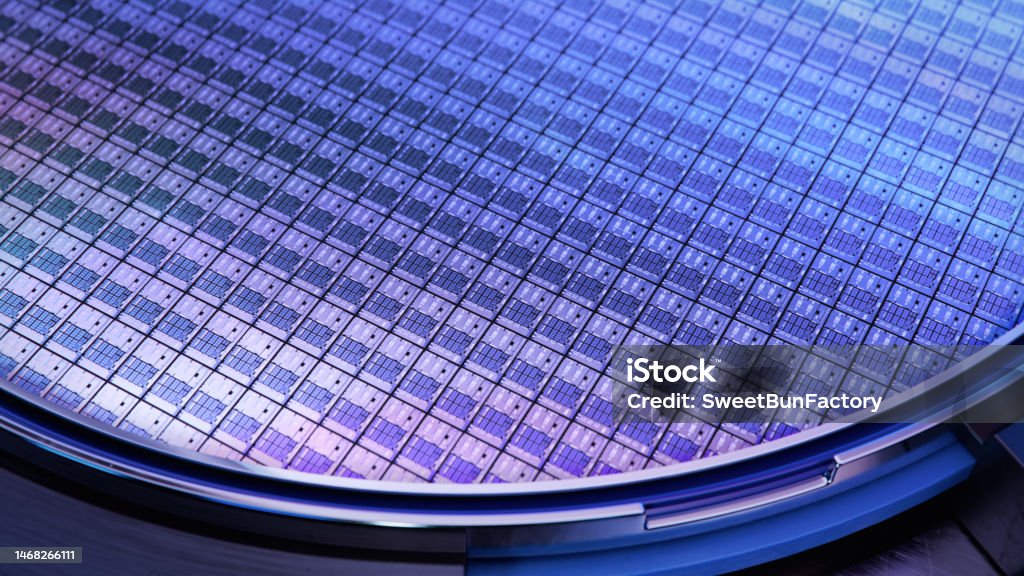
Semiconductor chips, in simple terms, involve miniaturizing circuits to the micron and nanometer levels, and embedding millions of PNP or NPN transistors that control 0s and 1s. Each transistor utilizes three endpoints—Gate, Source, and Drain—to control the formation of current channels. With shrinking optical lithography processes, the same-sized chips can accommodate more transistors, enhancing computational power and speed. This is akin to shrinking a vast electronic circuit the size of a football field down to the minuscule dimensions of the core chip in a smartphone, resembling a complex construction project involving layer upon layer of stacking and thousands of processes. However, it's impossible to shrink workers to fit inside the chip for flexible assembly of components. Hence, various semiconductor manufacturing equipments are used for chemical reactions. These reactions involve steps like CVD (Chemical Vapor Deposition) to deposit necessary materials, followed by grinding to absolute flatness, photolithography to apply photoresist according to design patterns, the etching machine removes the unnecessary parts through etching, subsequent cleaning for further processing, and then another run of different CVD for the next stage. Each layer's construction must be flawless to avoid defects that could impact yield rates. Otherwise, regrinding and remanufacturing may be required, with severe cases resulting in scrapping entire batches of wafers, leading to significant losses. The loss of approximately 25 pieces of 12-inch wafers in a box is comparable to losing a house, as each wafer contains hundreds or thousands of chips. In contrast to the simple ten-step process of PN junctions in solar panels, the design and manufacturing of semiconductor chips are highly intricate and complex. Even with substantial investment, it takes decades to mature and achieve over 95% yield rates in advanced semiconductor chip manufacturing.
As a side note on solar panels: In one end, purified silicon (with a valence of 4) mixed with a pentavalent element like phosphorus forms N-type silicon with an extra electron. On the other end, purified silicon (with a valence of 4) mixed with a trivalent element like boron forms P-type silicon with a deficit electron (similar to having an extra hole). Eventually, the electrons in N-type silicon absorb light energy, get excited, and become free electrons, generating current.
As a former semiconductor equipment application engineer, I had the opportunity to work in a cleanroom where we could only see each other's eyes. Using inspection tools like the Defect Review SEM (Scanning Electron Microscope), I examined memory cells on wafers that were approximately 0.1 micrometers in diameter, roughly equivalent to one-thousandth the width of a human hair. I also looked for various defects of the same size that could affect yield, such as voids, scratches, bumps, particles, bridges, and residue. It was both exciting and enlightening to understand how as semiconductor chips shrink according to Moore's Law, they approach physical limits where quantum effects become significant.
Moore's Law is the observation that the number of transistors on a microchip doubles approximately every two years, leading to a rapid increase in computing power and capabilities over time.
This can be simplified as follows: in today's nanoscale semiconductor devices, individual differences among a large group of people or electrons behaving like a wave or running in the same direction may seem negligible in the overall trend of conductivity. However, as transistors and other electronic components become smaller and approach atomic scales, quantum effects become more pronounced. Essentially, when there is only one person or one electron, even slight differences in movement or behavior become significant and cannot be ignored. Quantum effects exist beyond the binary states of 0 and 1, allowing for multiple states simultaneously. As a result, the computational power from multiple overlapping states becomes more powerful and faster.
In summary, while electron behavior in larger structures resembles waves, as the size approaches the nanoscale, quantum confinement effects may dominate, impacting the electronic properties of materials and devices.
At the nanoscale, the dimensions of materials become comparable to the wavelength of electrons, leading to quantum size effects. These effects can alter the electronic structure and conductivity of materials, potentially introducing challenges in maintaining reliable and predictable behavior of electronic devices. For instance, in traditional transistors, the switch states are well-defined, but at smaller scales, these states may become blurred due to quantum effects, thereby affecting the reliability and performance of the devices.
Quantum bits, or qubits, can exist simultaneously in multiple states within quantum superposition. When qubits are entangled, the states of the entangled qubits become intertwined. Measuring one qubit "collapses" its superposition, determining its state and instantaneously determining the state of the entangled qubits. Entanglement is a resource that realizes quantum parallelism. In classical computing, bits can be in states of 0 or 1. In quantum computing, qubits can exist in a superposition of both 0 and 1, and entanglement allows operations on combined states, providing potential advantages for certain types of computations. Quantum algorithms, such as quantum teleportation and quantum key distribution, harness entanglement to perform tasks that may be difficult or impossible with classical computing. Entanglement is a key aspect of quantum information processing. It is a resource that quantum computers can leverage to perform certain computations more efficiently than classical computers. It is a unique property of quantum systems and a core aspect of the potentially powerful performance of quantum computing in solving specific types of problems, such as large-number factorization, simulating quantum systems, and optimizing certain algorithms.
In the context of quantum mechanics, collapse refers to the sudden reduction of the wave function of a quantum system to one of its possible states when measured, resulting in the determination of the system's specific properties or state from a probabilistic distribution. It occurs typically when observing a quantum system, causing its properties or state to become definite.
Researchers and engineers in the semiconductor industry are actively exploring methods to mitigate or harness these quantum effects. This has led to the development of new materials, the design of novel device architectures, and exploration of quantum computing concepts to push the boundaries of classical computing based on Moore's Law. It's an exciting and evolving field of research, and the advent of quantum computing will have a revolutionary impact on the future of technology.
In 2023, Taiwan completed its first 5-qubit superconducting "quantum computer," housed in the "Quantum Computer Laboratory" in the basement of the Institute of Physics at the Academia Sinica. The core system of this laboratory is the "helium-3 helium-4 dilution refrigerator," which can maintain low temperatures for operation. It features multiple protective layers to shield highly sensitive quantum bits from external interferences such as magnetic fields. Currently, countries capable of independently developing and manufacturing superconducting quantum computers include the United States, China, Japan, the Netherlands, Finland, among others, which are few in number. The most advanced technology in this field is seen in the United States' IBM quantum computer, which has progressed to 433 qubits. However, they are now also developing a 133-qubit system, indicating that the number of qubits is just one aspect, and stable and efficient operation is crucial. Therefore, the number of qubits is not the most important factor, as even with a higher quantity, if the execution efficiency is low, it still requires a return to the starting point. Conversely, with high execution efficiency, one qubit can be equivalent to ten qubits in other systems. Although practical applications are still some distance away, similar to artificial intelligence, once successful, quantum computing will immediately bring about significant change.
The Jordan Harbinger Show919: Chris Miller | Chip War: The Battle for Semiconductor Supremacy
https://www.jordanharbinger.com/chris-miller-chip-war-the-battle-for-semiconductor-supremacy/
(With all transcript)
****** SOURCES & LINKS ******
* PlayerFM
https://player.fm/series/the-jordan-harbinger-show-2032122/ep-919-chris-miller-chip-war-the-battle-for-semiconductor-supremacy
* AEI Multimedia
https://www.aei.org/multimedia/the-jordan-harbinger-show-the-battle-for-semiconductor-supremacy/
(Chris Miller Twitter)
* iHeart Radio
https://www.iheart.com/podcast/867-the-jordan-harbinger-show-28966053/episode/919-chris-miller-chip-war-127776543/